Unlock innovation with Guru Solutions' expert PCB Design, Schematics, Gerbers & BOM services. We provide precise, reliable, and efficient solutions for your electronic projects, from concept to manufacturing. Get high-quality PCB layouts, detailed schematics, accurate Gerbers, and comprehensive BOMs for seamless product development.
Get Started
Ready to Innovate?
Transform Your Electronic Ideas into Reality with Guru Solutions
Guru Solutions provides end-to-end PCB Design, Schematics, Gerbers, and BOM Services, ensuring precision and reliability at every stage. Partner with us to streamline your electronic product development and achieve your design goals with confidence.
Our expert team at Guru Solutions is ready to craft high-quality PCB layouts, detailed schematics, accurate Gerber files, and comprehensive BOMs tailored to your unique specifications
From initial concept to manufacturing readiness, Guru Solutions is your trusted partner for superior PCB design and documentation. Let us handle the intricate details while you focus on your core business and accelerate your time to market.
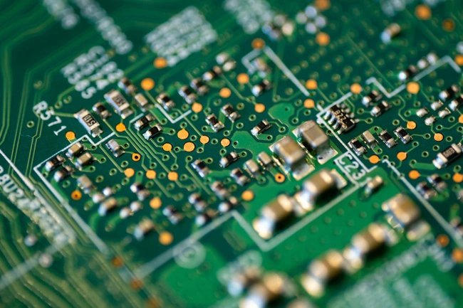
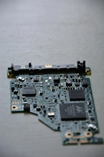
About Our PCB Design & Schematics & Gerbers & BOM Services
At Guru Solutions, we specialize in providing comprehensive and innovative PCB Design & Schematics & Gerbers & BOM Services. Our dedicated team of experienced engineers possesses a deep understanding of electronic circuit design principles, ensuring that every project, regardless of its complexity, is handled with utmost precision and expertise. We are committed to transforming your conceptual ideas into manufacturable and high-performing electronic products, utilizing the latest industry standards and advanced design tools to deliver solutions that exceed expectations. From initial circuit conceptualization to the final manufacturing files, we guide you through every step of the development process with clarity and technical proficiency.
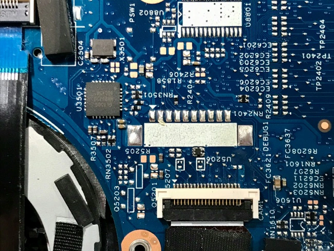
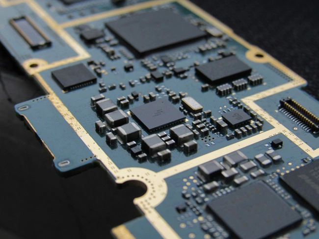
Our service offering is meticulously structured to cover every critical aspect of the electronic product development lifecycle. We begin with detailed schematic capture, meticulously laying out the electronic pathways and selecting the optimal components for your application. This foundational step is crucial for the overall functionality and performance of your device. Following schematic finalization, our focus shifts to sophisticated PCB layout design, where we strategically place components and route traces to optimize signal integrity, minimize noise, and ensure thermal efficiency. We understand that a well-designed PCB is not just about functionality but also about manufacturability and cost-effectiveness, and we strive to balance these crucial factors in every design.
Beyond the design phase, Guru Solutions provides comprehensive Gerber file generation and Bill of Materials (BOM) services. Our precise Gerber files are the industry standard for communicating design information to manufacturers, guaranteeing that your PCB can be produced accurately and efficiently. Simultaneously, our detailed BOMs provide a complete and organized list of all necessary components, streamlining your procurement process and preventing costly delays. We pride ourselves on delivering a complete package that facilitates a seamless transition from design to manufacturing, ensuring that your electronic product development journey is as smooth and efficient as possible from start to finish.

Altium Designer
Altium Designer is an industry-leading integrated PCB design software that provides a comprehensive suite of tools for schematic capture, PCB layout, and manufacturing outputs. Our proficiency in Altium Designer allows us to efficiently manage complex multi-layer designs, perform advanced routing, and conduct thorough design rule checks, ensuring the integrity and manufacturability of your electronic products. We leverage its powerful features for component management, signal integrity analysis, and 3D visualization, enabling us to create highly optimized and precise PCB designs that meet stringent performance requirements and accelerate your product development cycle with unparalleled accuracy and efficiency.

KiCad EDA
KiCad EDA is a powerful, open-source electronic design automation suite widely used for schematic capture and PCB layout. Our expertise in KiCad allows us to offer flexible and cost-effective design solutions without compromising on quality or functionality. We utilize its robust features for circuit simulation, footprint creation, and Gerber file generation, making it an excellent choice for a variety of projects, from simple prototypes to more complex designs. Our team leverages KiCad's extensive libraries and active community support to deliver efficient and reliable PCB designs, ensuring that your projects benefit from a highly capable and accessible design platform.

Eagle (Easily Applicable Graphical Layout Editor)
Eagle, now part of Autodesk Fusion 360, is a versatile PCB design software renowned for its intuitive interface and powerful capabilities in schematic capture and board layout. Our mastery of Eagle enables us to create intricate designs with precision and efficiency, supporting various board sizes and complexities. We utilize its comprehensive libraries, routing tools, and design rule checks to ensure optimal component placement and signal integrity, delivering high-quality PCB designs that are both functional and manufacturable. Our expertise in Eagle allows us to rapidly prototype and iterate designs, providing a flexible solution for your electronic product development needs.

SolidWorks PCB
SolidWorks PCB is a collaborative PCB design tool tightly integrated with SolidWorks mechanical design software, facilitating seamless communication between electrical and mechanical design teams. Our proficiency in SolidWorks PCB allows us to bridge the gap between electronic and mechanical engineering, ensuring that your PCB designs are perfectly aligned with mechanical enclosures and thermal considerations. We utilize its advanced features for component placement, routing, and 3D modeling, enabling us to identify and resolve potential interference issues early in the design process, leading to more efficient product development and a significantly reduced time to market for your complex electronic systems.
Enhancing Your Electronic Product Development
At Guru Solutions, we are dedicated to elevating your electronic product development journey through our specialized PCB Design & Schematics & Gerbers & BOM Services. The intricate process of transforming a conceptual idea into a tangible electronic device requires a meticulous approach, technical prowess, and a deep understanding of manufacturing nuances. Our team of seasoned engineers possesses this comprehensive skill set, ensuring that every design we produce is optimized for performance, reliability, and seamless integration into your broader product ecosystem. We prioritize clear communication and collaboration throughout the entire design lifecycle, guaranteeing that your vision is accurately translated into a robust and efficient electronic solution.
The foundation of any successful electronic product lies in the quality and precision of its underlying PCB design. We understand that errors at this stage can lead to costly delays and rework down the line. This understanding drives our commitment to delivering error-free schematics, meticulously routed PCB layouts, and accurate Gerber files. Our rigorous quality control processes and adherence to industry best practices ensure that your designs are not only technically sound but also comply with relevant regulatory standards. We empower you to mitigate risks associated with electronic hardware development, allowing you to focus your resources on innovation and market differentiation.
Ultimately, partnering with Guru Solutions for your PCB Design & Schematics & Gerbers & BOM needs means gaining a strategic advantage in a rapidly evolving technological landscape. We serve as your expert extension, providing the specialized knowledge and resources necessary to bring complex electronic products to fruition with efficiency and confidence. From simplifying your supply chain management with comprehensive BOMs to ensuring manufacturability with precise Gerber files, we are committed to providing a holistic service that accelerates your time to market and enhances the overall success of your electronic ventures.
"At Guru Solutions, we believe that exceptional electronic products are built on the bedrock of meticulous design. Our PCB Design, Schematics, Gerbers, and BOM Services embody our commitment to empowering innovation and transforming complex ideas into tangible realities for our clients."
Start Your Project Today
Guru Solutions offers unparalleled PCB Design & Schematics & Gerbers & BOM Services tailored to your unique needs. Our expert team is ready to provide precise, reliable, and efficient solutions, ensuring your next innovation is a resounding success
Streamlining Your Product Development Lifecycle
At Guru Solutions, our comprehensive PCB Design & Schematics & Gerbers & BOM Services are meticulously crafted to streamline your entire product development lifecycle. We understand that bringing a new electronic product to market involves numerous complex stages, and any inefficiencies can lead to significant delays and increased costs. By providing integrated solutions from initial concept to manufacturing readiness, we eliminate the need for you to coordinate with multiple vendors, thus simplifying your workflow and accelerating your time to market. Our holistic approach ensures seamless transitions between design phases, from schematic capture to final Gerber generation, ensuring consistency and accuracy throughout the entire process.
Our commitment to efficiency extends beyond just design; we also focus on optimizing for manufacturability from the very beginning. Our engineers employ Design for Manufacturability (DFM) principles throughout the PCB layout process, identifying and mitigating potential production issues before they arise. This proactive approach not only saves valuable time and resources during the manufacturing phase but also significantly reduces the likelihood of costly re-spins. By partnering with Guru Solutions, you gain the advantage of a design that is not only functionally superior but also inherently easier and more cost-effective to produce, leading to a smoother and more successful product launch.
Ultimately, our services empower your company to innovate faster and more reliably. By offloading the intricate and time-consuming tasks of PCB design, schematics, Gerber file creation, and BOM generation to our expert team, your in-house resources can focus on core competencies, strategic planning, and market analysis. This strategic partnership allows you to maximize your internal engineering bandwidth, accelerate your research and development efforts, and maintain a competitive edge in the rapidly evolving electronics industry. Let Guru Solutions be your trusted partner in bringing your next electronic innovation to life with unparalleled efficiency and expertise.


Cause
- Lack of In-House Expertise: Many companies may not have the specialized engineering talent required for complex PCB design, schematic capture, Gerber file generation, or BOM creation, necessitating external expert support.
- Accelerated Time-to-Market: To gain a competitive advantage, businesses need to bring new products to market quickly. Outsourcing these specialized services can significantly shorten design cycles.
- Cost-Effectiveness: Investing in dedicated software licenses, hardware, and training for an in-house PCB design team can be prohibitively expensive for many companies.
- Focus on Core Competencies: By entrusting PCB design and related tasks to specialists, companies can concentrate their internal resources on their primary business activities, such as innovation and strategic planning.
Benefits
- High-Quality, Reliable Designs: Our expertise ensures robust, optimized, and error-free PCB layouts, accurate schematics, and precise manufacturing files, leading to superior product performance.
- Reduced Development Costs: By leveraging our specialized tools, efficient processes, and experienced team, clients can avoid significant capital expenditures and reduce overall project costs.
- Faster Product Launch: Our streamlined design and documentation processes accelerate the development cycle, enabling clients to bring their products to market more quickly and capture opportunities.
- Improved Manufacturability: We incorporate Design for Manufacturability (DFM) principles, ensuring that designs are optimized for efficient and cost-effective production, minimizing manufacturing issues.
FAQ
Guru Solutions specializes in designing a wide range of PCBs, including single-sided, double-sided, and multi-layer boards, catering to varying complexities and applications. We serve diverse industries such as consumer electronics, industrial automation, medical devices, telecommunications, automotive, and IoT, adapting our design methodologies to meet specific industry standards and requirements for performance, reliability, and regulatory compliance.
We employ rigorous quality control procedures and utilize industry-standard tools to ensure the utmost accuracy of both Gerber files and BOMs. For Gerbers, we perform detailed Design for Manufacturability (DFM) checks to identify and correct any potential manufacturing issues before file generation. For BOMs, we meticulously cross-reference component data with schematics and industry databases, providing a comprehensive and error-free list to streamline your procurement and assembly processes.
Absolutely. Guru Solutions offers comprehensive support for revisions and modifications to existing PCB designs, schematics, Gerbers, and BOMs. Whether you need to update components, optimize layouts for new functionalities, improve performance, or address manufacturing issues, our experienced engineers can efficiently analyze your current design, implement necessary changes, and provide updated documentation, ensuring your product evolves seamlessly with your requirements.
Testimonial


Elevate Your Electronics
Partner with Guru Solutions for superior PCB Design & Schematics & Gerbers & BOM Services. Our commitment to quality, efficiency, and innovation ensures your project's success from concept to completion. Let us empower your next breakthrough.
How to Get it Done
We have a team of experts to help customize your software. Guru Solutions also offers a consultation service if you need advice on the software to use. We offer the best services at fair prices. Give us a call to schedule a meeting; invite us to your office or even home, and we will be there.